
Magic-Angle Twisted Bilayer Graphene – Yes, That’s The Scientific Name

In the world of physics research, graphene has been gaining popularity as one of the most remarkable materials in the last 15 years. While it may appear unassuming in common household goods such as pencil leads, the material boasts a higher strength than steel and a higher flexibility than paper. On top of all that, it is also ultra-light and an excellent conductor of electric current and heat.

Recently, physicists from the Massachusetts Institute of Technology discovered that stacking two sheets of graphene and twisting a small angle between them reveals an entire new field of material science – twistronics. In a paper published in Nature, researchers have taken a look into this new material, known as the magic-angle twisted bilayer graphene. By modifying the graphene’s temperature, they were able to cause the material to shift from behaving like an insulator to transforming into a superconductor.

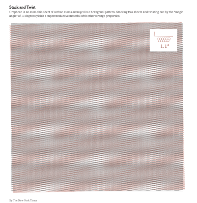
A graphic in the New York Times demonstrates some of the interesting properties that arise from stacking and twisting two sheets. Scientists have long known that graphene is a one-layer-thick honeycombed pattern of carbon atoms, but actually separating a single sheet of graphene has been fairly difficult. A low-tech method pioneered by two physicists at the University of Manchester involves using sticky tape to pull apart graphene layers until a single layer is left.

Small imperfections that arise from slightly misaligned sheets manifests in a pattern that allows electrons to hop between atoms in regions where the lattice line up, but unable to flow in regions that are misaligned. The slower moving electrons are thus more likely to interact with each other, becoming “strongly correlated”.

The technique for measuring the properties of this new twisted graphene is similarly low-tech. After a single layer of graphene is separated by sticky tape, the tape is torn in half to reveal two halves with perfectly aligned lattices. One of the sides is rotated by about 1.3 degrees and pressed onto the other. Sometimes, the layers would snap back into alignment, but other times they would end up at 1.1 degrees and stop rotating.

When the layers were cooled to a fraction of a degree above absolute zero, they were observed to become a superconductor, an incredibly discovery for the physicists involved in the experiment. Further studies showed that different permutations of temperature, magnetic field, and electron density were also able to turn the graphene into a superconductor. On top of this, the graphene was also able to exhibit a form of magnetism arising from the movement of electrons rather than the intrinsic properties of the atoms. With so many possibilities still unexplored, it’s certain that twistronics will reveal some remarkable findings pretty soon.

[Thanks Adrian for the tip!]


from Hackaday https://ift.tt/2t7MJO7

Comments

Popular posts from this blog

How To Play Doom – And More – On An NES

Doom was a breakthrough game for its time, and became so popular that now it’s essentially the “Banana For Scale” of hardware hacking. Doom has been ported to countless devices, most of which have enough processing ability to run the game natively. Recently, this lineup of Doom-compatible devices expanded to include the NES even though the system definitely doesn’t have enough capability to run it without special help. And if you want your own Doom NES cartridge, this video will show you how to build it . We featured the original build from [TheRasteri] a while back which goes into details about how it’s possible to run such a resource-intensive game on a comparatively weak system. You just have to enter the cheat code “RASPI”. After all the heavy lifting is done, it’s time to put it into a realistic-looking cartridge. To get everything to fit in the donor cartridge, first the ICs in the cartridge were removed (except the lockout IC) and replaced with custom ROM chips. Some modifica...

The Flexible Permanence of Copper Tape Circuits

Somewhere between shoving components into a breadboard temporarily and committing them to a piece of protoboard or a PCB lies the copper tape method. This flexible Manhattan-style method of circuitry formed the basis for [Bunnie Huang]’s Chibitronics startup, and has since inspired many to stop etching boards and start fetching hoards of copper tape. [Hales] hit the ground running when he learned about this method , and has made many a copper tape circuit in the last year or so. He offers several nice tips on his site that speak from experience with this method, and he’ll even show you how to easily work an SMD breakout board into the mix. Generally speaking, [Hales] prefers plywood as the substrate to paper or cardboard for durability. He starts by drawing out the circuit and planning where all the tape traces will go and how wide they need to be. Then he lays out copper traces and pads, rubs the tape against the substrate to make it adhere strongly, and reinforces joints and laps w...

The Newbie’s Guide To JTAG

Do you even snarf? If not, it might be because you haven’t mastered the basics of JTAG and learned how to dump, or snarf, the firmware of an embedded device. This JTAG primer will get you up to snuff on snarfing, and help you build your reverse engineering skills. Whatever your motivation for diving into reverse engineering devices with microcontrollers, JTAG skills are a must, and [Sergio Prado]’s guide will get you going. He starts with a description and brief history of the Joint Test Action Group interface, from its humble beginnings as a PCB testing standard to the de facto standard for testing, debugging, and flashing firmware onto devices. He covers how to locate the JTAG pads – even when they’ve been purposely obfuscated – including the use of brute-force tools like the JTAGulator . Once you’ve got a connection, his tutorial helps you find the firmware in flash memory and snarf it up to a file for inspection, modification, or whatever else you have planned. We always apprec...